Document Type : Original Research Article
Authors
1 Department of Physics and Industrial Physics, Faculty of Physical Sciences, Nnamdi Azikiwe University, Awka, Nigeria
2 Department of Physics and Astronomy, Faculty of Physical Sciences, University of Nigeria, Nsukka, Enugu State, Nigeria
3 National Centre for Physics, Quaid-i-Azam University Campus, Islamabad, Pakistan
Abstract
Zirconium doped Lead selenide (PbSe) nanocrystal films were synthesized on FTO substrates by electrodeposition technique, and analyzed by UV-Visible Spectrophotometer, four-point probes technique, scanning electron microscopy (SEM), X-ray diffractometer and Energy dispersive X-ray analysis (EDX). The results show that the synthesized Zr/PbSe films exhibited an increase in optical absorbance as the deposition pH increased, with the highest absorbance value in the UV region. The forbidden energy gap values of the synthesized films were observed to increase with an increase in deposition pH. A direct forbidden energy gap ranging from (1.80–1.90)eV within the pH value of 7.5–9.0 was recorded. A refractive index range of 0.65-1.25 was observed. The XRD patterns show that the synthesized films exhibit large grain size and polycrystalline and cubic crystal structure. The SEM image exhibits a densely packed uniformed smooth surface of distribution of spherical-shaped grains, which covered the entire substrate. The spherical-shaped-like grains coalesce to form bigger particles with triangular-shaped rough surfaces at a higher value of pH. The film thicknesses were found to decrease from 105.55nm to 100.98nm as the pH increased from 7.5 to 9.0.
Keywords
Main Subjects
Introduction
Chalcogenide semiconductor nanostructured materials have gained significant interest in photovoltaic (PV) technologies applications because of their expected favorable economic fabrication approach and their optoelectronic properties. Chalcogenide materials exhibit unique device efficiency by inactivating the defect in the absorber layer, tailoring the interfacial carrier transport layer, and bandgap engineering [1]. Chalcogenide semiconductor material mostly displayed narrow optical band gap properties suitable for thermoelectric devices, infrared detectors, and lasers [2].
Among those chalcogenide semiconductors, PbSe semiconductors have received great attention from many researchers during the last few decades due its non-toxic and earth-abundant materials with high absorption coefficient (> 105 cm-1) and optimal forbidden energy gap range of (1- 1.5eV) for photovoltaic absorber layer [3]. PbSe semiconductors also exhibit properties suitable in optoelectronic devices like LEDs, optical fibers, semiconductor lasers, and solar cells mostly because of their stability under ambient conditions and multiple exciton generation effects that enhance photocurrent [4].
These unique and interesting optical, morphology, structural, and electrical properties of PbSe semiconductors can be modulated by their deposition technique and varying their deposition parameters to give desired applications [5]. Having control over the deposition parameters by manipulation of grain size and morphology can consequently allow for tuning of the forbidden energy gap from 0.27ev to as far as 2.0ev. [6]. Many researchers have prepared pure PbSe films through several methods such as chemical bath deposition [7, 8, 9,10,11], electrodeposition [11, 12], sputtered deposition [13], thermal evaporation [5], RF magnetron sputtering [14], etc. In comparing with the above, the electrochemical method put forward unique and great advantages in synthesizing chalcogenide semiconductor nanostructured materials such as the ability to control the structures, shapes, and sizes of the electrodeposits, economic viability, easy scalability, and desired purity of the end product [15].
The control of deposition condition such as bath pH is an important factor and play a crucial role in the determination of morphology, and structural, optical, and electrical properties of the deposit. Previously, the work of [16] reported the change in the forbidden energy gap from 3.56 to 1.4 eV as a result of a change in pH value for the PbSe thin film. [17] also reported a decrease in the forbidden energy gap as the pH increases for nanostructured PbSe thin films [18-25, 26-29]
This paper reports on the influence of solution pH on the optical, structural, electrical, and morphological properties of electrochemically synthesized zirconium-doped PbSe semiconductor nanostructure material to determine the optimal condition process for photovoltaic application.
Experimental details: Synthesis of zirconium-doped PbSe thin films
The Zr-doped PbSe thin films were electrochemically deposited on fluorine-doped tin oxide (FTO) glass slides. Preceding the actual deposition, the FTO glass substrates were first cleaned with acetone and methanol for 20 and 7 minutes respectively. It was then removed and rinsed with purified laboratory distilled water and stored appropriately in a clean glass jar to decontaminate the substrate surfaces. High-purity reagents were used in the preparation of all the solutions with purified laboratory distilled water. High-purity reagents were used in the preparation of all the solutions with purified laboratory distilled water. The precursors used were lead (II) nitrate Pb(NO3)2, zirconium (IV) oxide chloride octahydrate (Cl2OZr·8H2O), selenium (IV) oxide (SeO2), and Ammonia (NH3). Lead (II) nitrate Pb(NO3)2 and selenium (IV) oxide (SeO2) were used as sources of cation and anion respectively. Zirconium (IV) oxide chloride octahydrate (ZrCl₂.8H₂O) was used as a dopant precursor and Ammonia (NH3) was used to vary the pH of the reaction bath. The Zr/PbSe aqueous electrolytic solution was prepared by measuring 20 mL of 0.1M solution of Pb(NO3)2 and 10 mL of 0.01M solution of SeO2 using an electronic scale machine into a 100 mL beaker. 0.01M solution of Cl2OZr8H2O, representing the dopant concentration was added into SeO2 and Pb(NO3)2 100 mL beaker. A magnetic stir plate was used to stir the complete mixture for 10 minutes to attain an equivalent mixture. the pH of the reaction bath was varied as 7.50, 8.00, 8.50, and 9.00 with the addition of an appropriate amount of Ammonia (NH3) while the dopant concentration and temperature were kept constant as shown in Table 1. The prepared reaction bath was connected through the carbon electrode and FTO substrate to the power supply. The deposited films were subjected to annealing at 400°C.
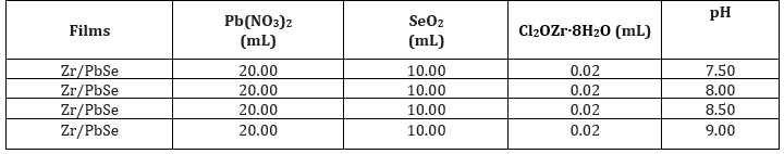
Table 1: Variation of deposition pH for Zr/PbSe films
The synthesized Zr/PbSe films were subjected to various characterizations. D8-Advance X-ray diffractometer with Cu-Kα radiation (K1=1.5406Å) was used to examine the structural properties of the films. EDX and SEM techniques were used to study the chemical composition and surface morphology properties respectively for the synthesized films. The optical properties were examined using the 756S UV-visible spectrophotometer.
Optical properties of Zr/PbSe films
The influence of pH variation on the absorbance spectra of Zr/PbSe films is shown in Figure 1a. It revealed that the absorbance values of the synthesized Zr/PbSe films decrease across the UV-VIS-NIR region of the spectrum in a similar pattern for all the samples as the deposition pH increases, with the film sample deposited at pH value of 9.0 exhibiting the maximum value of absorbance in the UV region of the spectrum. The plot also revealed that the film deposited at a pH value of 7.5 indicated a minimum value of absorbance in the UV region. This trend indicated that the film's absorbance increases with an increase in solution pH. The maximum absorbance value exhibited in the UV region shows the potential applications of the synthesized films in solar cell fabrication [18]. Figure 1b displayed the plot of transmittance against wavelength for Zr/PbSe films at different deposition pH. The transmittance values increase with an increase in the wavelength of the incident radiation for the deposited Zr/PbSe films. The film deposited at a pH value of 8.5 displayed the highest transmittance value in the visible region, while the film sample deposited at a pH value of 8.0 had the lowest transmittance value in the UV region of the spectrum. The trends indicate an increase in transmittance values with an increase in solution pH of the Zr/PbSe films. The high value of transmittance in the visible region suggests that the films would be used for window glaze materials and optical absorbers in solar cells [19]. The reflectance spectra for the Zr/PbSe films are shown in Figure 1c. The reflectance values first increase with the increase in pH, reaching maximum value within the UV region. A further increase in pH leads to a decrease in the reflectance value across the VIS-NIR region with the sample deposited at a pH value of 8.5 exhibiting the lowest value of reflectance. This low value of reflectance for the Zr/PbSe films in the VIS-NIR region makes it applicable for anti-reflection coating [20]. To determine the influence of pH variation on the band gap property of the deposited samples, the linear part of the plot of absorption coefficient square against photon energy was extrapolated to photon energy. Figure 1d revealed that the optical band gap value first decreases from 1.80 eV to 1.70 eV as the pH value increases from 7.5 to 8.0. A further increase in pH value to 8.5 resulted in an increase in band gap energy to 1.90 eV. It can be observed that the increase in solution pH of the deposited samples increased the optical direct band gap of the deposited Zr/PbSe films. The band gap energy ranged from 1.80 eV to 1.90 eV within the pH value of 7.5 to 9.0. Similar trends was reported by [21].
The plot of the refractive index against photon energy is shown in Figure 2a. The plot indicates that the value of the refractive index for all the deposited samples first increases with an increase in pH until it reaches a maximum value and falls sharply with the sample deposited at pH value of 8.0 having the lowest value of the refractive index. The refractive indexes were almost constant for the films deposited at pH of 8.5 and 9.0 within the photon energy of 1.8 eV to 1.9 eV. Figure 2b shows the plot of extinction coefficient against photon energy for Zr/PbSe films at different deposition pH. It revealed that the sample with a pH value of 8.0 exhibited the highest value of extinction coefficient. Increasing the value of pH shifts the value of the extinction coefficient lower in a similar pattern for all samples. Figure 2c illustrates the plot of optical conductivity of the synthesized Zr/PbSe films at different pH. The plot showed that the optical conductivity increased toward higher photon energy as the pH increased. The value of the real dielectric constant of the deposited films first rises with the increase in deposition pH, reaches a maximum value within the range of 1.8 -1.9 eV, and then decreases toward higher photon energy for all samples as shown in Fig. 3a&b. The imaginary dielectric constant of the deposited films increases with deposition pH.
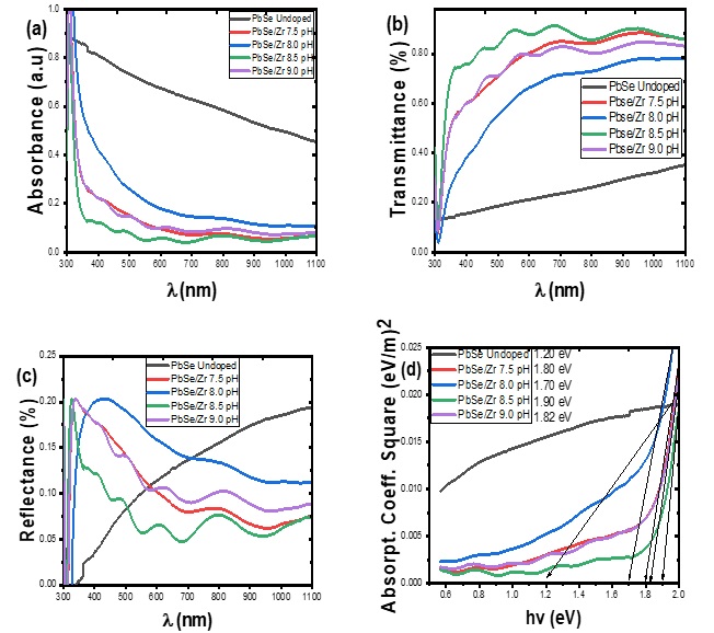
Figure 1: Plot of absorbance (a), transmittance (b), reflectance (c) absorption coefficient square (d) against wavelength and photon energy for undoped PbSe and PbSe/Zr films at different deposition pH.
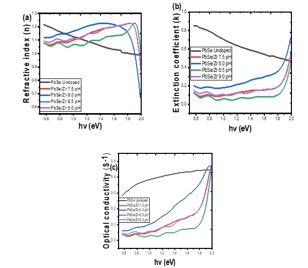
Figure 2: Plot of refractive index (a), extinction coefficient (b), and optical conductivity (c) against photon energy for undoped PbSe and PbSe/Zr films at different deposition pH.
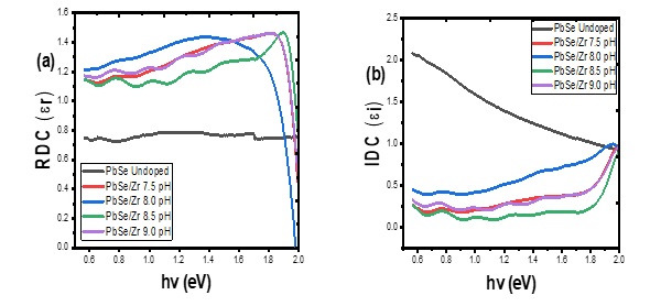
Figure 3: Plot of real (a) and imaginary (b) dielectric constant against photon energy for undoped PbSe and PbSe/Zr films at different deposition pH.
Structural properties of Zr/PbSe films different deposition pH
Figure 4 shows the XRD patterns for Zr/PbSe films at different deposition pH. The pattern revealed the films crystallized with five strong diffraction peaks at (220), (112), (310), (202), and (212) directions with corresponding 2θangles of (26.409), (33.752), (38.075), (51.834), and (65.901). These values of diffraction peaks were confirmed with standard X-ray data (JCPD No: 00-004-0688) to give cubic structure. The narrow nature of the diffraction patterns indicates large grain size and polycrystalline. The diffraction pattern also revealed that there were no notable changes in the diffraction's intensity peak as deposition pH increased. The intensity of the diffractogram is low for all samples and is attributed to the small thickness of the film [22]. The other structural parameters like the lattice constant, crystallite size, and dislocation density were calculated and are shown in Table 2. It revealed that the lattice constant of the synthesized Zr/PbSe films decreases with an increase in the value of deposition pH. It can be observed that the grain size of the synthesized samples first increased from 0.69136 nm to 0.99107 nm with an increase in the deposition's value pH from 7.5 to 8.0. A further increase in the deposition pH to 8.5 resulted in the reduction of grain size to 0.68261 nm. The value of the grain size further increased to 0.73443nm as the value of deposition pH increased to 9.0. This result is justified by the SEM micrograph image obtained in Figure 5 for the synthesized films. The sample deposited at a pH value of 8.5 produced the highest dislocation density value of 6.45804 while that of pH value of 8.0 resulted in the lowest dislocation density value of 3.0926
Surface morphology and chemical composition of Zr/PbSe films at different pH
The SEM micrographs of the synthesized Zr/PbSe films at different deposition pH are shown in Figure 5. The figure revealed an even distribution of hollow grains of nano sizes with spherical shapes on the smooth surface. As the deposition pH increased to 8.0, the spherical-shaped grains coalescence to form bigger particles with triangular shapes with rough surfaces. The increase in grain size as the deposition increases would be a result of an increase in the rate of hydrolysis and condensation [23]. At a pH value of 8.5, the SEM image exhibits a densely packed uniformed smooth surface of distribution of spherical shaped-like grains, which covered the entire substrate. A further increase in pH value to 9.0 yielded a sparse, random distribution of spherical shaped grains with well-defined boundaries. The long chains of grains and the defined grain boundaries exhibited by the synthesized Zr/PbSe films indicate structural homogeneity [24]. The porosity of the synthesized materials enhanced high charge transport resistance by reducing particle-particle inter-conductivity and increasing grain boundary density [25].
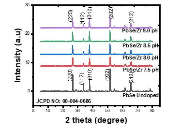
Figure 4: XRD pattern for Zr/PbSe films at different deposition pH.
Table 2: Structural parameters of PbSe and PbSe/Zr films
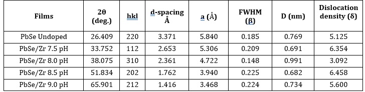
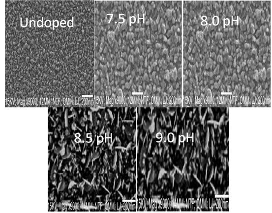
Figure 5: SEM micrographs for Undoped and PbSe/Zr films at different deposition pH.
Electrical analysis of Zr/PbSe films with different pH
Table 3 represents the summarized electrical properties of PbSe and Zr/PbSe films showing resistivity, electrical conductivity, and thickness deposited at different pH. The table shows that the resistivity of the synthesized films decreases as the deposition pH increases. The electrical conductivity of the synthesized films increases as the deposition pH increases. The value of the electrical conductivity ranged from (1.61 x 10⁻⁶ to 1.36 x 10⁻⁶) (Ω.m)-1 which falls within the 10-12 to 102 (Ω.m)-1 electrical conductivity value for semiconductor material as the pH [18]. These indicate that the pH plays a significant role in influencing the resistivity and electrical conductivity of the deposited films. The observed range of electrical resistivity (6.20 x 10⁻⁵ to 7.30 x 10⁻⁵)Ω.m1 for the synthesized films indicates the materials can be deployed for buffer layer fabrication in enhancing conversion efficiency of solar radiation. Figure 6a&b shows the plot of pH variation as a function of thickness for Zr/PbSe at different pH. The plot revealed that thickness decreases from 105.55 nm to 100.98 nm as the pH increases from 7.5 to 9.0.
Table 3: Electrical properties of PbSe and PbSe/Zr
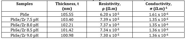
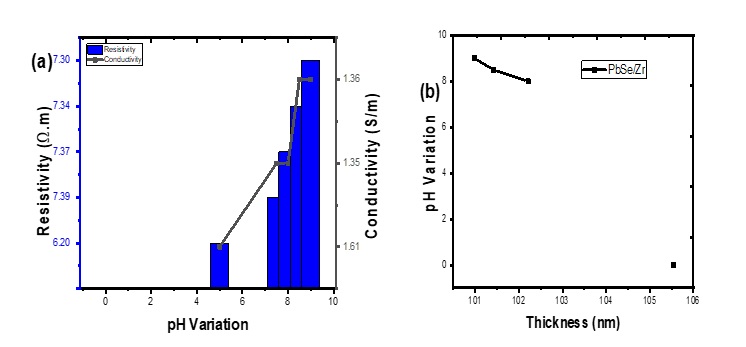
Figure 6: resistivity and conductivity as a function of pH variation(a) thickness(b).
Conclusion
Zr/PbSe films were successfully synthesized on FTO substrates using an electrodeposition technique with the variation of deposition pH values. The effects of the pH variation on the morphology, structural, optical, and electrical properties of electrochemically synthesized Zr/ PbSe material and their photovoltaic application were studied. The optical analyzes of the synthesized films verified the effect of pH variation and it has been found that increasing the pH values increased the optical band gap of the synthesized films. The absorbances of the films were found to increase with the increase in pH. High values of transmittance in the visible region were recorded and suggest that the films would be used for window glaze materials and optical absorbers in the solar cells. However, the diffraction pattern of the synthesized films revealed there were no notable changes in the diffraction's intensity peak as deposition pH increased. The lattice constant of the synthesized Zr/PbSe films decreases with an increase in the value of deposition pH. The SEM micrographs illustrate the increased and changes in the shape of the grains as the pH values increased.
Conflicts of Interest
No conflicts of interest to report
Data Availability Statement The corresponding author can provide the data that backs up the study's findings upon request.
ORCID
Imosobomeh L. Ikhioya : 0000-0002-5959-4427
)